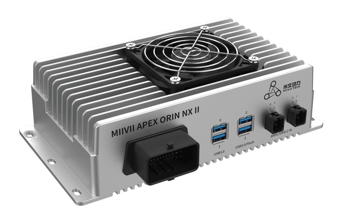
APEX ORIN NX II GPIO Digital Input#
Hardware Connection#
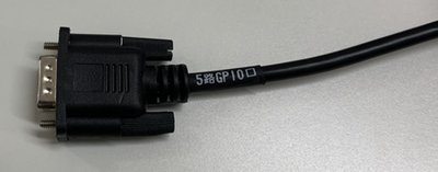
Interface Pin Definition#
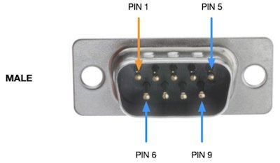
Connector |
DB9 Pin Number |
Description |
Utility Channel Index |
|---|---|---|---|
DI_0 |
1 |
GPIO IN |
0 |
DI_1 |
2 |
GPIO IN |
1 |
DO_0 |
3 |
GPIO OUT |
0 |
DO_1 |
4 |
GPIO OUT |
1 |
GND |
6-9 |
Ground |
Connector |
DB9 Pin Number |
Description |
Utility Channel Index |
|---|---|---|---|
DI_2 |
1 |
GPIO IN |
2 |
DI_3 |
2 |
GPIO IN |
3 |
DO_2 |
3 |
GPIO OUT |
2 |
DO_3 |
4 |
GPIO OUT |
3 |
GND |
6-9 |
Ground |
Use this channel index with the DI or DO utility shown below.
DI Hardware Specifications#
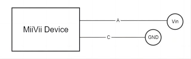
The rated DI operating range is 0–24 V. The permitted input range (Vin) is 0–48 V. The permitted input range is distinct from the product’s rated operating range.
Electrical indicators |
Specification |
|---|---|
Vin Range |
0~48V |
Logical High (Output Logical 1) |
2.4V≤Vin≤48V |
Logical Low (Output Logical 0) |
0V≤Vin≤1.2V |
IO Speed |
≤100KHz |
Peer interface requirements |
The series resistance of the peer interface to GND is less than 1KΩ |
DI Usage#
GPIO usage examples are shown below
sudo /opt/miivii/features/gpio/bin/miivii_get_di_value <DI number>

# <DI number>: DI index; 0 for DI0, 1 for DI1, and so on.
# The command returns the current DI logic level: 0 for low, 1 for high.
# Example: read the input of di0
# sudo /opt/miivii/features/gpio/bin/miivii_get_di_value 0
Compile the Sample Code
cp -r /opt/miivii/features ~/
cd ~/features/gpio
sudo make;
GPIO Troubleshooting#
1. Permissions and Pin Ownership#
Symptom |
Possible Cause |
Solution |
|---|---|---|
Running the message |
GPIO is already in use by another driver or process |
1. Check what is using the pin: 2. Terminate the process using the pin: 3. Force release: |
Accessing |
The user is not in the |
1. Add the user to the group: 2. Change file permissions: |
2. Abnormal Logic Levels#
Symptom |
Possible Cause |
Solution |
|---|---|---|
Unstable Output Level |
1. Power supply interference or poor grounding 2. A PCB signal trace crosses a split plane, causing an impedance discontinuity<br>3. Load current exceeds the limit |
1. Add decoupling capacitors for filtering 2. Check PCB routing and avoid signal traces crossing split power planes 3. Use an external MOSFET to drive high-current loads |
Incorrect Input Value |
1. Pull-up or pull-down resistors are not configured 2. External voltage is outside the allowable range |
1. Configure a pull-up in software: 2. Add a 4.7kΩ pull-up resistor or use a level shifter |
System Hangs When Reading the Level in Output Mode |
1. Incorrect access to the input data register (IDR) 2. A short circuit in the external circuit |
1. Read the state from the output data register instead 2. Add a 100Ω series current-limiting resistor to prevent overcurrent |
3. Interrupt and Event Detection Issues#
Symptom |
Possible Cause |
Solution |
|---|---|---|
Interrupt Does Not Respond(edge triggering fails) |
1. Incorrect interrupt type configuration 2. ISR blocks for too long |
1. Confirm the trigger edge: 2. Optimize the ISR: use |
False Event Detection(for example, a high-level event is triggered unexpectedly) |
1. Signal noise 2. Poor solder joint or contact at the pin |
1. Add software debouncing: in 2. Use shielded cable to reduce interference or add an RC filter |
4. Function Configuration Conflicts#
Symptom |
Possible Cause |
Solution |
|---|---|---|
GPIO Direction Setting Does Not Take Effect(cannot switch between input and output) |
1. Pin multiplexing conflict, such as a pin assigned to I2C 2. Driver is not loaded |
1. Check the device tree: confirm that 2. Load the driver: |
Switching the Same Pin between Output and Input Fails |
1. Mode switching timing conflict 2. Interrupt preemption causes inconsistent state |
1. Perform the operation with interrupts disabled: 2. Cache the state in a global variable to avoid frequent switching |